 sasa11
Nov 22,2013
581
sasa11
Nov 22,2013
581
Ink materials for printed circuit boards (PCBs)
DuPont Microcircuit Materials (MCM) has developed a broad and growing portfolio of CB Series screen printed ink materials for rigid and flexible printed circuit boards (PCBs). Current offerings inclu...
sasa11
Nov 22,2013
391
circut board
Stands for "printed circuit board." A PCB is a thin board made of fiberglass, composite epoxy, or other laminate material. Conductive pathways are etched or "printed" onto board, connecting different ...
sasa11
Nov 21,2013
703
Single Sided Mixed Technology Reflow Process
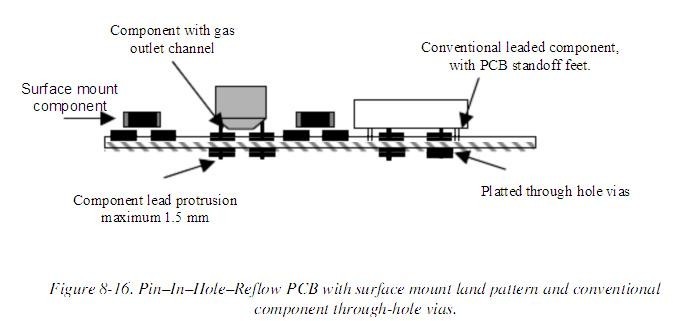
A relatively new procedure has been developed to enable a single reflow operation to solder both surface mount and conventional through-hole components on the same board. This is particularly desirabl...
sasa11
Nov 21,2013
1651
Mixed Technology PCB Assembly
There are still components that are not available in surface mount configuration (for example, some connectors and capacitors). Therefore, some assemblies have through-hole and surface mount component...
sasa11
Nov 21,2013
2635
Double Sided PCB Assembly and Soldering
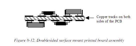
To achieve higher component density, the double-sided assembly technology has evolved. Double-sided circuit boards have copper tracking and component pads (land pattern) on the top and bottom side of...
sasa11
Nov 21,2013
3382
Wave (Flow) Soldering Process
Since the introduction of automated PCB assembly and component lead soldering, wave soldering has been the mainstream method of applying solder automatically to the bottom side of PCBs. Wave soldering...
sasa11
Nov 21,2013
856
PCB assembly enters reflow process
Since the introduction of automated PCB assembly and component lead soldering, wave soldering has been the mainstream method of applying solder automatically to the bottom The PCB is passed though the...
sasa11
Nov 21,2013
406
Re-flow Soldering Process
Reflow soldering is the making of solder joints by (re) melting previously applied solder, usually in the form of a paste. A re-flow machine is a conveyorised oven that transports the pasted and compo...
sasa11
Nov 21,2013
353
Single Sided Surface Mount PCB Assembly
Single sided PCB assembly requires components to be assembled on only one side of the circuit board and is the least complex of PCB surface mount assembly processes. Double sided and variants of surfa...
sasa11
Nov 21,2013
670
Solder Pasting and Printing (surface mount process)
To achieve accurate positioning of components, surface mount assembly PCBs must be designed to ensure that component pad (land pattern) dimensions and layout are in accordance with good practice and t...
sasa11
Nov 21,2013
1096
Component Placement onto the Printed Circuit Board
The best-expected manual insertion rate of through-hole components is 200 to 400 components per hour. Automation has been a prime objective for printed circuit board assemblers since the electronics i...
sasa11
Nov 21,2013
349
Printed Circuit Board Designs
Fundamentally, there are two PCB design systems - through hole and surface mount. In through-hole process, components have connecting pins that are pushed through plated holes (vias) in the PCB and pr...
sasa11
Nov 20,2013
332
Surface-mount circuitry-PCB
Surface-mount circuitry of the PCBs does not require a hole for each component lead. Automated testing, however, may require vias on every node. The holes were never an issue with through-hole circuit...
sasa11
Nov 20,2013
367
Through-Hole Considerations-PCB
The older technology for op amps and other components is through-hole. Components are constructed with leads that insert through holes in the board hence the name. Through-hole components, due to th...
sasa11
Nov 20,2013
2830
PCB Trace-to-Plane Capacitance Formula
For example, if the capacitance formula is applied to the following trace: 4 Layer board signal routing next to ground planeBoard layer thickness: 0.188 mmTrace Width: 0.75 mmTrace Length: 7.5 mm A ...
sasa11
Nov 20,2013
385
Trace Reflections-PCBs
Reflections and matching are closely related to loop antenna theory, but different enough to warrant their own discussion. When a PCB trace turns a corner at a 90 angle, a reflection can occur. This i...
sasa11
Nov 20,2013
351
Board Stack-Up The Order of Layers
There has been a lot of confusion in the past over what is the optimum order for PCB layers. Take, for example, a 4-layer board consisting of two signal layers, a power plane, and a ground plane. Is i...
sasa11
Nov 20,2013
339
Multi-Layer PCBs
Double-sided boards, in spite of their benefits, are not the best method of construction, especially for sensitive or high-speed designs. The most common board thickness is 1.5 mm. This separation is ...
sasa11
Nov 20,2013
314
Single-Sided PCBs
Very simple consumer electronics are sometimes fabricated on single-sided PCBs, keep-ing the raw board material inexpensive (FRC1 or FRC2) with thin copper cladding. These designs frequently include m...
sasa11
Nov 20,2013
320
PC Board materials Materials Choosing the Right One for the Application
PC Board materials are available in various grades, as defined by the National Electrical Manufacturers Association (NEMA). It would be very convenient for designers if this organization was closely a...
| Ranking | Name | Answers |
|---|


